


The core packaging processes of AET
- Categories:Company News
- Author:
- Origin:
- Time of issue:2022-01-25 16:17
- Views:
The core packaging processes of AET
- Categories:Company News
- Author:
- Origin:
- Time of issue:2022-01-25 16:17
- Views:
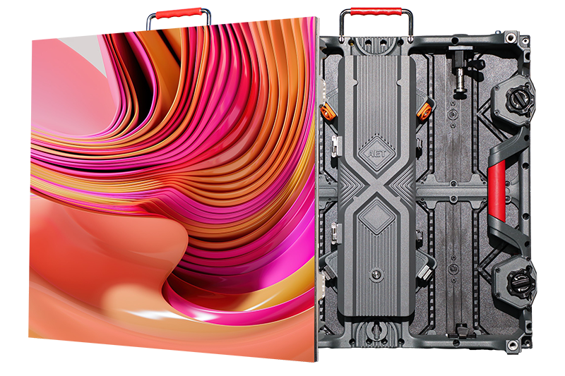
There is a place in AET, which is very secretive, it is called the “Shield of AET”. It is the place where AET 's unique weapons are forged.What kind of “weapons”do AET have?What are the advantages of them?How does AET use these “weapons”? AET patented packaging technology is our secret “weapons”,we are going to explore one by one in this article.
AOB(Admixture on Board)
Lamp beads are completely sealed inside the matte transparent protective layer by using the insulated high molecular materials.It is done by using the semiconductor automation equipment with AET’s unique packaging technology.AOB technology allows the contact ability of LED and PCB to be more sensitive,so that graininess of lights can be diminished.
Advantages of AOB technology: with this mature technique,high yield can be achieved,as well as uniformity and color consistency is increased. The angle range of light emitted from the lamp beads are expanded to 170°,moire phenomenon are diminished.LED displays are waterproof,dust-free,anti-collision due to this unique technology.Display effect is being greatly improved, screens are more reliable,cost of maintenance is being reduced as a result.
BOB(Bi-Layer on Board)
BOB technology is an upgraded version of AOB,it is a self developed new type of surface light-emitting technology,we called it surface optical treatment.Improved the level of protection of LED display as well as its displaying effect to suit customer’s different needs.It lay a good foundation for the future expansion of the application field of LED display.
Advantages of BOB technology:on top of the AOB technology,products with BOB technology have better and softer display effect because the interference between lamp panel are avoided.Pictures are fuller and vivid as the moire phenomenon are disappeared due to this technology.Highly transparent and with greater hardness,the splicing become more precise.Protection against water,dust and collision are increased,so the LED displays are even more reliable.
The breakthrough of AET’s own patented AOB and BOB packaging technology could solve the technical bottlenecks and the limitation of usage of packaging.High quality products and better display effect are the results of our patented packaging technology.These could maximize the value of Micro spacing display and reflect higher cost performance.
AET Application of patented packaging technology
AET does not stop here,we upgraded our own patented core packaging BOB technology to QCOB packaging technology by adding comprehensive quantum dot technique.AT series products are the first of LED display industry to use this QCOB technique.Display effect,evenness of displays and cost performance are all being improved compared with the traditional products with COB packaging technology.
Information on AT series:
International standard sizes:43〃,46〃,55〃,60〃
Equilibrium brightness:0~1000nits
Color depth:18bit
Viewing angle:170°
Max frame frequency:120fps
Max refresh rate:3840Hz
Display ration:16:9
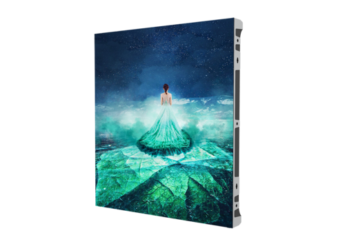
Characteristics:Ultra-wide color gamut and contrast rate;rich in color,delicate quality of display picture;higher protection level;seamless splicing;immersive effect can be achieved.
Applications:Broadcasting,monitoring centers,conference hall,shopping mall,school and sports event etc.
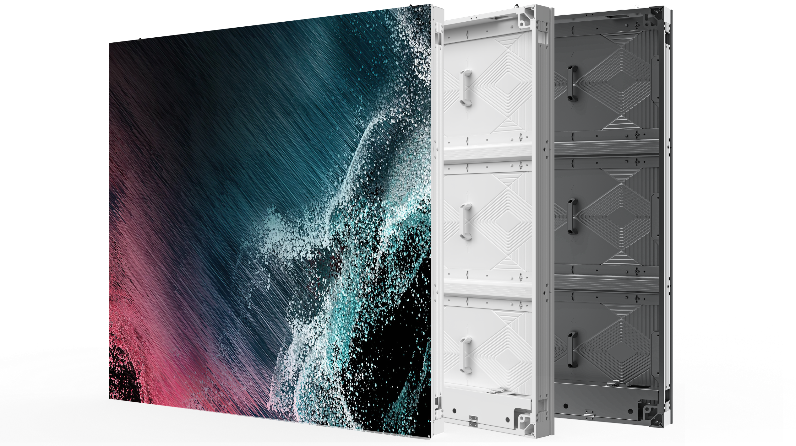
Besides the independently developed patented AOB and BOB packaging technologies,COB technology and N in 1 SMT technology are still being used in AET to give our customers more choices,to create more value for our customers too.These two packaging technologies have their own advantages.
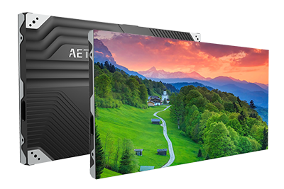
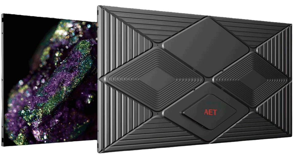
AET packaging technology
COB packaging technology
Advantages:
total flip chip;no welding wire is needed;high yield;common cathode driven power supply mode for lower heat dissipation and better energy-saving effect;production efficiency as a result of more chips can be packaged once;protection against static and collision;lower failure rate of the bead due to the covered pins;small volume for Micro spacing(below P1.0)
N in 1 SMT packaging technology
Advantages:
The strength of anti-collision is higher because the the size of the single lamp bead is bigger;Faulty pins are less due the higher patching efficiency and less solder joints.
“Shield of AET” is not only a place where its our own patented packaging technology is being developed, but also an important part of AET's process of building an ultra-high definition LED display ecosystem.This department is the “armor”for the LED display system,it has protocols, equipped with advanced technology and working closely with other department.AET always keep in mind the vision of “ being the excellent creator of Micro spacing LED displays”,and we spare no effort to walk with you on this journey of Micro spacing display!
NEWS


 Annual General Conference")
CONTACT
9-10th Floor , 1st Building, E Zone, Guangda We Valley, 4th Keji Road, Songshan Lake High-tech Industrial Development Zone, Dongguan City, Guangdong Province,China
SUBSCRIBE
Subscribe To Our Newsletter


Copyright 2022 @ AET Displays Limited All Rights Reserved. 粤ICP备19077615号 Sitemap Support:300.cn Dongguan SEO